- 您现在的位置:买卖IC网 > Sheet目录287 > 25C040X/ST (Microchip Technology)IC EEPROM 4KBIT 3MHZ 8TSSOP
�� �
�
�25AA040/25LC040/25C040�
�3.5�
�Read� Status� Register� (RDSR)�
�3.6�
�Write� Status� Register� (WRSR)�
�The� RDSR� instruction� provides� access� to� the� STATUS�
�register.� The� STATUS� register� may� be� read� at� any� time,�
�even� during� a� write� cycle.� The� STATUS� register� is�
�formatted� as� follows:�
�The� WRSR� instruction� allows� the� user� to� select� one� of�
�four� levels� of� protection� for� the� array� by� writing� to� the�
�appropriate� bits� in� the� STATUS� register.� The� array� is�
�divided� up� into� four� segments.� The� user� has� the� ability�
�7�
�X�
�6�
�X�
�5�
�X�
�4�
�X�
�3�
�BP1�
�2�
�BP0�
�1�
�WEL�
�0�
�WIP�
�to� write-protect� none,� one,� two,� or� all� four� of� the�
�segments� of� the� array.� The� partitioning� is� controlled� as�
�illustrated� in� Table� 3-2.�
�The� Write-In-Process� (WIP)� bit� indicates� whether� the�
�25XX040� is� busy� with� a� write� operation.� When� set� to� a�
�See� Figure� 3-7� for� WRSR� timing� sequence.�
�‘� 1� ’,� a� write� is� in� progress,� when� set� to� a� ‘� 0� ’,� no� write� is�
�in� progress.� This� bit� is� read-only.�
�TABLE� 3-2:�
�ARRAY� PROTECTION�
�The� Write� Enable� Latch� (WEL)� bit� indicates� the� status�
�of� the� write� enable� latch.� When� set� to� a� ‘� 1� ’,� the� latch�
�allows� writes� to� the� array,� when� set� to� a� ‘� 0� ’,� the� latch�
�prohibits� writes� to� the� array.� The� state� of� this� bit� can�
�always� be� updated� via� the� WREN� or� WRDI� commands�
�regardless� of� the� state� of� write� protection� on� the�
�STATUS� register.� This� bit� is� read-only.�
�The� Block� Protection� (BP0� and� BP1)� bits� indicate�
�which� blocks� are� currently� write-protected.� These� bits�
�are� set� by� the� user� issuing� the� WRSR� instruction.� These�
�BP1�
�0�
�0�
�1�
�1�
�BP0�
�0�
�1�
�0�
�1�
�Array� Addresses�
�Write-Protected�
�none�
�upper� 1/4�
�(0180h-01FFh)�
�upper� 1/2�
�(0100h-01FFh)�
�all�
�(0000h-01FFh)�
�bits� are� nonvolatile.�
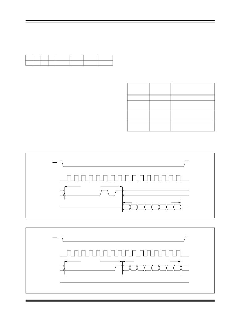
�See� Figure� 3-6� for� RDSR� timing� sequence.�
�FIGURE� 3-6:�
�CS�
�READ� STATUS� REGISTER� SEQUENCE�
�0�
�1�
�2�
�3�
�4�
�5�
�6�
�7�
�8�
�9�
�10�
�11�
�12�
�13�
�14�
�15�
�SCK�
�Instruction�
�SI�
�0�
�0�
�0�
�0�
�0�
�1�
�0�
�1�
�SO�
�High-impedance�
�7�
�Data� from� STATUS� register�
�6� 5� 4� 3� 2� 1�
�0�
�FIGURE� 3-7:�
�CS�
�WRITE� STATUS� REGISTER� SEQUENCE�
�0�
�1�
�2�
�3�
�4�
�5�
�6�
�7�
�8�
�9�
�10�
�11�
�12�
�13�
�14�
�15�
�SCK�
�Instruction�
�Data� to� STATUS� register�
�SI�
�0�
�0�
�0�
�0�
�0�
�0�
�0�
�1�
�7�
�6�
�5�
�4�
�3�
�2�
�1�
�0�
�High-impedance�
�SO�
�DS21204E-page� 10�
�?� 2006� Microchip� Technology� Inc.�
�发布紧急采购,3分钟左右您将得到回复。
相关PDF资料
25C080-I/P
IC EEPROM 8KBIT 3MHZ 8DIP
25C320-E/P
IC EEPROM 32KBIT 3MHZ 8DIP
25LC010AT-E/MC
IC EEPROM 1KBIT 10MHZ 8DFN
25LC040AT-E/MC
IC EEPROM 4KBIT 10MHZ 8DFN
25LC080A-I/STG
IC EEPROM 8KBIT 10MHZ 8TSSOP
25LC1024T-E/MF
IC EEPROM 1MBIT 20MHZ 8DFN
25LC128-E/MF
IC EEPROM 128KBIT 10MHZ 8DFN
25LC160/P
IC EEPROM 16KBIT 2MHZ 8DIP
相关代理商/技术参数
25C040X-E/P
制造商:MICROCHIP 制造商全称:Microchip Technology 功能描述:4K SPI ⑩ Bus Serial EEPROM
25C040X-E/SN
制造商:MICROCHIP 制造商全称:Microchip Technology 功能描述:4K SPI ⑩ Bus Serial EEPROM
25C040X-E/ST
功能描述:电可擦除可编程只读存储器 512x8 - 5V Rot Pin RoHS:否 制造商:Atmel 存储容量:2 Kbit 组织:256 B x 8 数据保留:100 yr 最大时钟频率:1000 KHz 最大工作电流:6 uA 工作电源电压:1.7 V to 5.5 V 最大工作温度:+ 85 C 安装风格:SMD/SMT 封装 / 箱体:SOIC-8
25C040X-EST
制造商:未知厂家 制造商全称:未知厂家 功能描述:SPI Serial EEPROM
25C040X-I/P
制造商:MICROCHIP 制造商全称:Microchip Technology 功能描述:4K SPI ⑩ Bus Serial EEPROM
25C040X-I/SN
制造商:MICROCHIP 制造商全称:Microchip Technology 功能描述:4K SPI ⑩ Bus Serial EEPROM
25C040X-I/ST
功能描述:电可擦除可编程只读存储器 512x8 - 5V Rot Pin RoHS:否 制造商:Atmel 存储容量:2 Kbit 组织:256 B x 8 数据保留:100 yr 最大时钟频率:1000 KHz 最大工作电流:6 uA 工作电源电压:1.7 V to 5.5 V 最大工作温度:+ 85 C 安装风格:SMD/SMT 封装 / 箱体:SOIC-8
25C040X-I/STG
功能描述:电可擦除可编程只读存储器 512x8 - 5V Rot Pin Lead Free Package
RoHS:否 制造商:Atmel 存储容量:2 Kbit 组织:256 B x 8 数据保留:100 yr 最大时钟频率:1000 KHz 最大工作电流:6 uA 工作电源电压:1.7 V to 5.5 V 最大工作温度:+ 85 C 安装风格:SMD/SMT 封装 / 箱体:SOIC-8